Semiconductor Innovation Advances Toward 3D Architectures as Measurement Capabilities Lag Behind
Insights from National Physical Laboratory highlight a growing gap between chip design complexity and the ability to validate next-generation semiconductor systems.
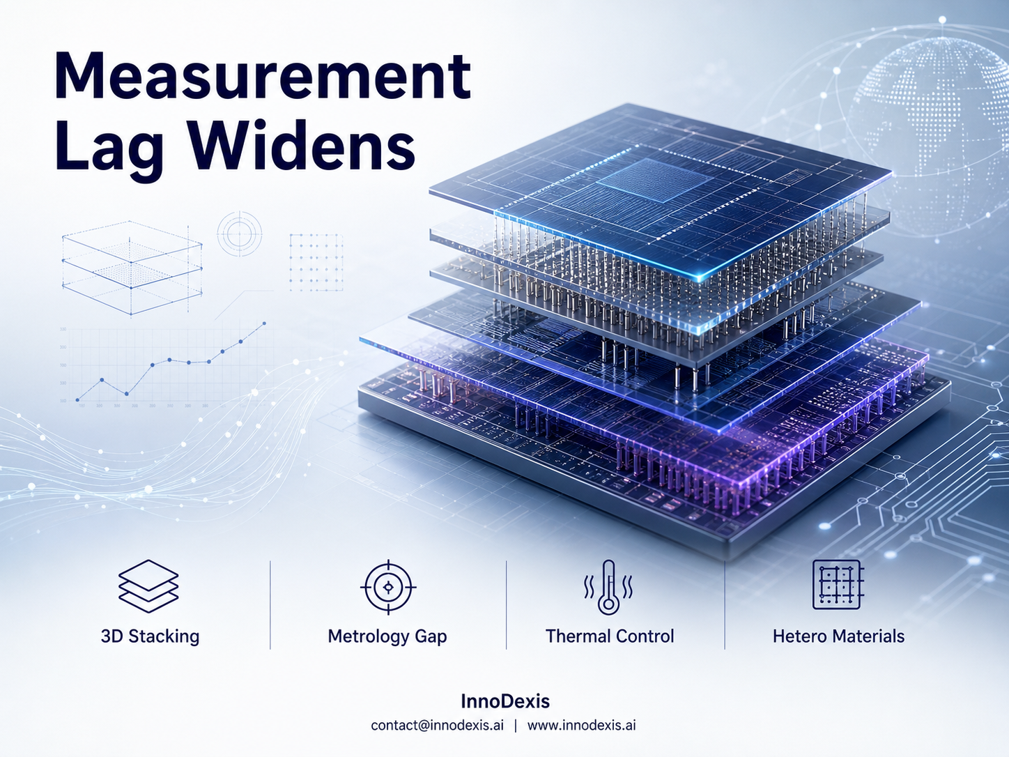
InnoDexis has published its latest Innovation Intelligence Report covering semiconductor innovation, analyzing emerging developments in chip design, materials, and validation frameworks. The report reveals that as semiconductor systems transition toward complex 3D-stacked architectures and new material integrations, measurement capabilities are not advancing at the same pace. Insights from National Physical Laboratory indicate that while design innovation continues to expand, the ability to reliably measure and validate next-generation systems is becoming a critical constraint.
Key Findings
Semiconductor design is shifting from traditional two-dimensional scaling toward complex three-dimensional stacked architectures. This transition increases system density and performance potential but introduces new challenges in alignment, thermal management, and interconnect complexity that require advanced validation methods.
Demand from artificial intelligence, 6G networks, and high-performance computing is accelerating the need for more advanced semiconductor systems. These application domains require higher processing capabilities and data throughput, further intensifying the pressure on both design and validation frameworks.
New materials are being introduced into semiconductor stacks, including two-dimensional semiconductors, diamond-based heat dissipation layers, and compound photonics components. These materials expand performance capabilities but also introduce measurement complexities due to their distinct physical and thermal properties.
Measurement limitations are becoming more visible as system complexity increases. Current tools face challenges in verifying nanometre-scale alignment across multiple stacked layers, understanding heat behavior in ultra-dense environments, and accurately assessing data movement constraints commonly referred to as the “memory wall.”
Pre-standards research is emerging as a key activity area, driven by national laboratories and industry collaborations. This phase focuses on defining measurement approaches and validation frameworks before formal standardization, indicating a proactive effort to address gaps in current metrology capabilities.
Strategic Insight and Trend Analysis
The findings indicate a structural shift in the semiconductor industry, where the limiting factor is no longer solely design capability but the ability to measure and validate increasingly complex systems. As architectures evolve beyond planar scaling into vertically integrated and heterogeneous configurations, traditional metrology approaches are becoming insufficient.
The integration of diverse materials and components into a single system amplifies this challenge. Each material introduces unique physical behaviors that must be measured with precision to ensure system reliability and performance. Without corresponding advances in measurement science, the ability to scale these innovations into production environments becomes constrained.
The rise of pre-standards research suggests that industry and national institutions are recognizing measurement as a foundational requirement for future semiconductor progress. By establishing early validation frameworks, stakeholders aim to reduce uncertainty and enable smoother transitions from research to commercialization.
This shift repositions metrology from a supporting role to a central component of semiconductor innovation. Measurement is increasingly linked to trust, reproducibility, and scalability. As a result, control over measurement frameworks and standards may influence which technologies reach market readiness and which remain constrained at the research stage.
Global and Industry Implications
For corporates and R&D teams, the findings highlight the need to integrate measurement considerations early in the design process. Developing advanced semiconductor systems may require parallel investment in metrology capabilities to ensure that innovations can be validated and scaled effectively.
For investors and capital allocators, the emergence of measurement as a bottleneck suggests potential opportunities in metrology technologies, validation platforms, and standards development initiatives. These areas may become increasingly important as enabling layers for semiconductor advancement.
For policymakers and national innovation bodies, the growing importance of measurement and standards indicates a strategic domain for national competitiveness. Supporting metrology research and pre-standards development may play a critical role in shaping future semiconductor ecosystems and ensuring technological sovereignty.
InnoDexis Statement
“The current trajectory of semiconductor innovation indicates that measurement and validation frameworks will play a defining role in determining which technologies can scale from design to deployment,” noted InnoDexis in its latest intelligence report.
Conclusion
The semiconductor landscape is entering a phase where advances in architecture and materials are outpacing the tools required to validate them. As demand from AI, 6G, and high-performance computing continues to grow, the ability to measure complex systems with precision will become increasingly critical. The transition toward measurement and standards leadership reflects a broader shift in how innovation is evaluated and scaled. The complete Semiconductor Innovation Intelligence Report is available to InnoDexis subscribers and enterprise clients.
About InnoDexis
InnoDexis is a global Innovation Intelligence platform that tracks, analyzes, and interprets breakthrough innovations, prototypes, and emerging technologies across industries and countries. Its intelligence helps corporates, investors, and policymakers understand the true structure and direction of global innovation. Learn more at innodexis.ai.