International Team Achieves First Experimental Realization of an All-Optical Photonic Time Crystal, Extending Light Control Into the Time Domain
Researchers from Germany and France have demonstrated the world's first all-optical photonic time crystal, modulating optical properties on picosecond timescales and reducing photon dissipation within the metamaterial by half.
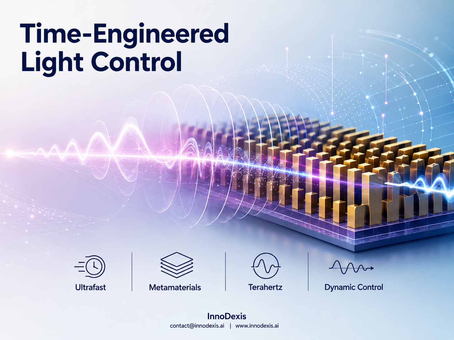
InnoDexis has published its latest Innovation Intelligence Report covering photonic materials and ultrafast optical engineering, analyzing a world-first experimental innovation developed across institutions in Germany and France. The report reveals that an international research team from HZDR, École polytechnique, Collège de France, and Thales has experimentally realized the first all-optical photonic time crystal — a plasmonic metamaterial modulated on picosecond timescales using ultrafast terahertz laser pulses — opening a previously inaccessible dimension of optical engineering in which light properties are controlled dynamically in the time domain rather than through fixed physical structure.
Key Findings
The experimental realization of the world's first all-optical photonic time crystal represents a domain boundary crossed rather than an incremental performance improvement. Photonic crystals have historically shaped light through fixed spatial structure; this innovation extends the same principles into the time domain, enabling on-demand tuning of light properties at speeds previously out of experimental reach. The result was independently confirmed by a theoretical model developed alongside the experimental study.
The device was built from micrometer-scale gold crenellated structures over an indium-antimony semiconductor — a plasmonic metamaterial architecture that enabled optical property modulation on picosecond timescales comparable to the light's own oscillation cycle. This timescale equivalence is significant: modulation at speeds approaching the oscillation period of light itself represents a qualitatively different regime of optical control from anything achievable through static material design.
Temporal modulation of the metamaterial reduced photon dissipation within the device by half. This finding carries direct implications for the next phase of the research programme, which targets further photon dissipation reduction and amplification as steps toward a new class of terahertz laser. A 50% reduction in dissipation at the first experimental demonstration establishes a meaningful baseline for what temporal modulation can achieve in this material system.
The terahertz frequency range in which the photonic time crystal operates sits in a recognised gap between electronic and photonic systems — a spectral region that has historically been underserved by both device classes. Dynamic optical control at picosecond timescales in the terahertz range positions photonic time crystals as a candidate technology for bridging this gap, with potential relevance for optical computing and advanced telecommunications applications.
The experimental methodology — using ultrafast terahertz laser pulses to drive temporal modulation — opens a dimension of optical engineering that fixed material design cannot access. Where conventional photonic engineering is constrained by the physical structure of a fabricated device, temporal modulation enables properties to be changed on demand without altering the underlying material, representing a structural shift in how optical systems can be designed and operated.
Strategic Insight and Trend Analysis
The strategic significance of this innovation is best understood as the opening of a new engineering dimension rather than an advance within an existing one. Photonic crystal engineering has operated for decades within the constraint that light control is achieved through spatial structure — the geometry, periodicity, and composition of a fabricated material. That constraint is now experimentally lifted.
The implications of this shift compound over time. Once a new control dimension is experimentally validated, the engineering community gains access to a design space that was previously theoretical. Every optical system that currently relies on static photonic structure — from waveguides to resonators to filters — becomes a candidate for reimagining with temporal modulation as an additional degree of freedom. The question is no longer whether temporal control of light is possible but how rapidly the engineering community can develop the tools, materials, and architectures to exploit it.
The terahertz gap context is particularly strategically relevant. The frequency range between roughly 0.1 and 10 terahertz has remained difficult to address because electronic devices are too slow and conventional photonic devices are not well matched to the wavelengths involved. A device class that operates natively in this range through temporal modulation — and that has already demonstrated 50% photon dissipation reduction at first demonstration — represents a credible candidate for addressing a long-standing gap in the electromagnetic spectrum coverage of practical device technologies.
The next stated research targets — further dissipation reduction and amplification — are the two capabilities required for a functional laser. If achieved, a terahertz laser class built on photonic time crystal principles would represent a commercially significant outcome from what is currently a fundamental physics demonstration.
Global and Industry Implications
For corporates and R&D teams in photonics, semiconductor, and telecommunications sectors, the photonic time crystal demonstration signals a new design dimension that will require monitoring as it develops toward application readiness. Teams working on terahertz imaging, sensing, and communications infrastructure have the most immediate strategic interest, as the device operates natively in the frequency range most relevant to next-generation terahertz system development.
For investors and capital allocators, the innovation is at an early fundamental stage with a clearly articulated development roadmap toward terahertz laser functionality. The four-institution international collaboration — spanning Germany and France — indicates a well-resourced foundational research effort. The translational timeline is long-term, but the combination of a world-first experimental result and a defined next-phase target provides a more structured investment signal than early-stage photonics work typically offers.
For policymakers and national innovation bodies, the collaboration between HZDR, École polytechnique, Collège de France, and Thales demonstrates the value of cross-institutional and cross-border research partnerships in achieving experimental firsts that no single institution could reach independently. The terahertz gap has strategic relevance for defence, communications, and sensing — domains where national capability building in foundational photonics carries long-term significance.
InnoDexis Statement
"The experimental realization of a photonic time crystal extends optical engineering into the time domain for the first time, opening a design space that static material architectures cannot access and establishing a foundational platform for a new class of terahertz devices," noted InnoDexis in its latest intelligence report.
Conclusion
The first experimental realization of an all-optical photonic time crystal marks the opening of a new chapter in optical engineering — one in which dynamic temporal control complements the spatial control that has defined photonic device design for decades. As the research programme advances toward photon amplification and terahertz laser development, and as the broader photonics community begins to explore temporal modulation as a design tool, the implications for optical computing, telecommunications, and terahertz sensing will become increasingly concrete. InnoDexis will continue to track developments in photonic time crystals, metamaterial engineering, and terahertz device technology. The complete Photonic Time Crystal Innovation Intelligence Report is available to InnoDexis subscribers and enterprise clients.
About InnoDexis
InnoDexis is a global Innovation Intelligence platform that tracks, analyzes, and interprets breakthrough innovations, prototypes, and emerging technologies across industries and countries. Its intelligence helps corporates, investors, and policymakers understand the true structure and direction of global innovation. Learn more at innodexis.ai.